Vacuum pneumatic chuck: "sub-micron" precision tool for semiconductor manufacturing
The global chip industry faces the dual challenges of wafer thinning limit (3nm process thickness ≈ 0.1mm) and yield improvement bottleneck (defect density needs to be <0.01/cm²). Traditional robotic arms are severely limited in development due to micro-stress damage (yield loss exceeding 5%) and uncontrollable cleanliness (Class 1 environmental particulate rate exceeding the standard by 18%). Vacuum pneumatic chucks have become the key to breaking through physical limits through nano-scale contact surfaces and intelligent static dissipation. The semiconductor automation market is expected to reach $89.2 billion by 2025 (according to Gartner's forecast), and the penetration rate of vacuum technology is projected to exceed 70%.
Technological breakthroughs in four core scenarios
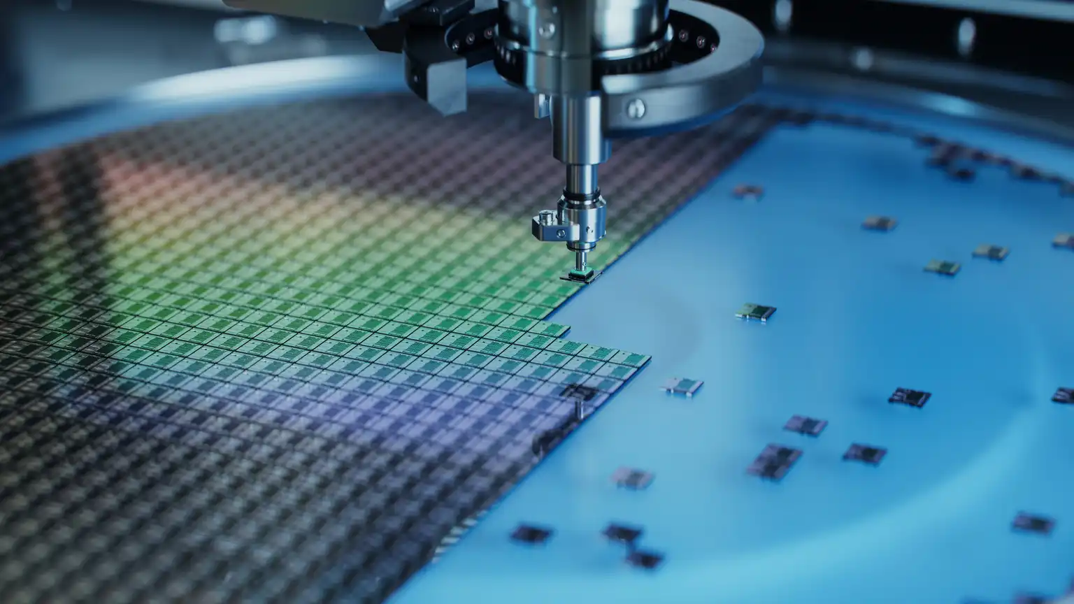
- Wafer transfer: Ultra-thin silicon wafers can be transported without damage
Industry pain points: The breakage rate of 300mm wafers during manual handling is >2%, and micro-cracks cause losses of $2.3 billion per year (SEMI 2025 report).
Asian efficiency-enhancing design:
▶ Anti-voltage fluctuation system (±25% grid adaptability)
▶ Fast-change module (product switching <45 seconds)
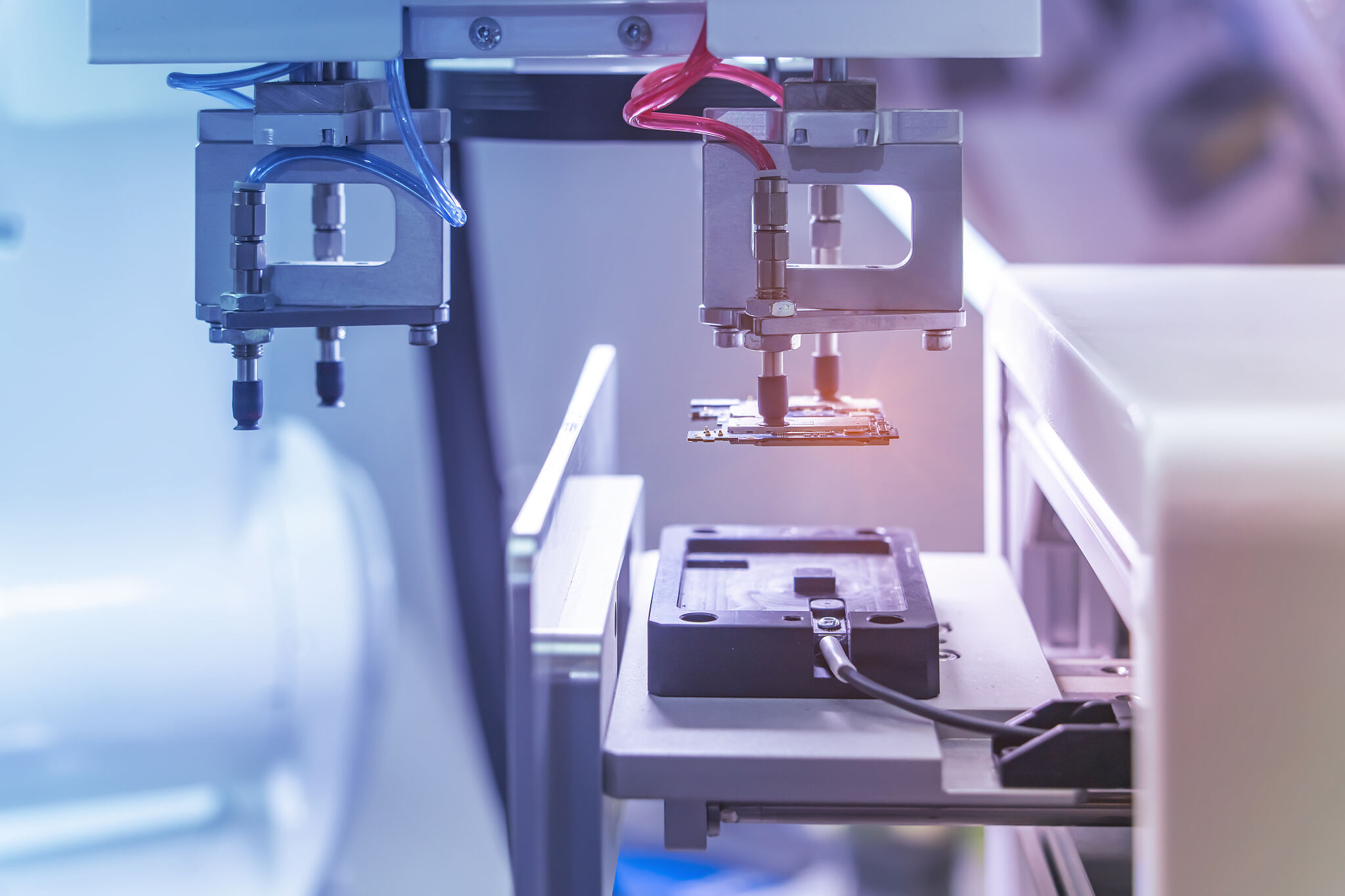
2. Chip mounting: sub-micron precision positioning
Technology revolution:
Traditional solution defects: mounting offset ±5μm, thermal deformation leading to cold solder joints, ESD damage rate 0.8%.
Vacuum suction cup solution: visual compensation positioning accuracy ±0.1μm, real-time temperature compensation (ΔT<0.1℃) reduced to 0.05%.
3. Packaging test: Stable operation in extreme environments.
Disruptive value:
Chemical corrosion-resistant material: Resistant to etching liquid/acid mist (lifespan > 500,000 cycles).
High-temperature adaptive system: Accuracy maintained at ±1μm in 300℃ reflow soldering environment.
Global cases:
TSMC 3nm production line: yield rate increased to 99.95%.
Malaysia packaging and testing plant: The investment payback period is only 8 months.
Cost savings:
Fragmentation losses reduced by 90%.
Maintenance costs reduced by 40%.
Installation speed increased by 35%.
Yield increased to 99.98%.
Avoided $120 million in ESD losses per year.